- 您现在的位置:买卖IC网 > Sheet目录1994 > DS3105LN+ (Maxim Integrated Products)IC TIMING LINE CARD 64-LQFP
DS3105
16
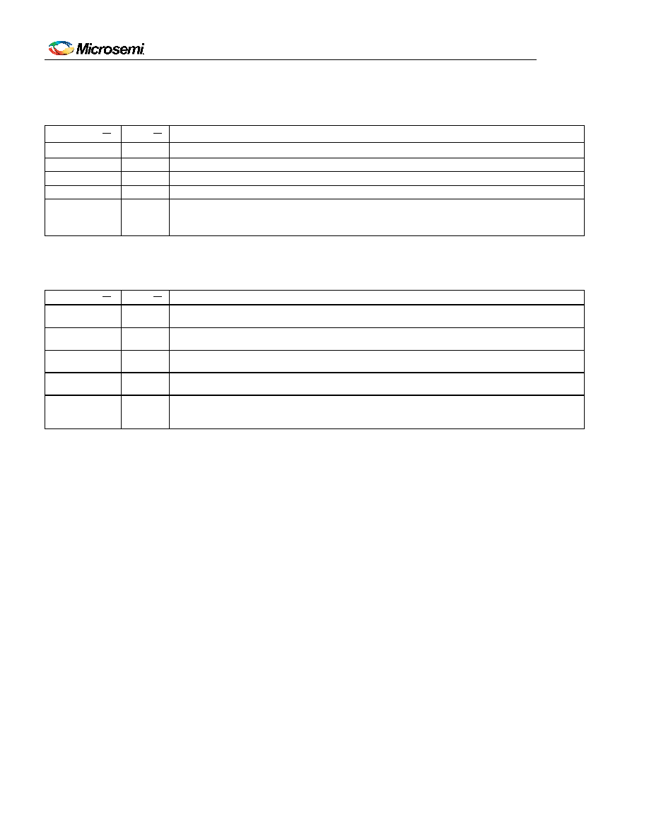
Table 6-4. SPI Bus Mode Pin Descriptions
PIN NAME
TYPE
PIN DESCRIPTION
CS
IPU
Chip Select. This pin must be asserted (low) to read or write internal registers.
SCLK
I
Serial Clock. SCLK is always driven by the SPI bus master.
SDI
I
Serial Data Input. The SPI bus master transmits data to the device on this pin.
SDO
O
Serial Data Output. The device transmits data to the SPI bus master on this pin.
CPHA
I
Clock Phase. See Figure 7-4.
0 = Data is latched on the leading edge of the SCLK pulse.
1 = Data is latched on the trailing edge of the SCLK pulse.
Table 6-5. JTAG Interface Pin Descriptions
PIN NAME
TYPE
PIN DESCRIPTION
JTRST
IPU
JTAG Test Reset (Active Low). Asynchronously resets the test access port (TAP) controller. If
not used,
JTRST can be held low or high.
JTCLK
I
JTAG Clock. Shifts data into JTDI on the rising edge and out of JTDO on the falling edge. If
not used, JTCLK can be held low or high.
JTDI
IPU
JTAG Test Data Input. Test instructions and data are clocked in on this pin on the rising edge
of JTCLK. If not used, JTDI can be held low or high.
JTDO
O3
JTAG Test Data Output. Test instructions and data are clocked out on this pin on the falling
edge of JTCLK. If not used, leave unconnected.
JTMS
IPU
JTAG Test Mode Select. Sampled on the rising edge of JTCLK and is used to place the port
into the various defined IEEE 1149.1 states. If not used connect to VDDIO or leave
unconnected.
发布紧急采购,3分钟左右您将得到回复。
相关PDF资料
DS3106LN+
IC TIMING LINE CARD 64-LQFP
DS3231MZ+
IC RTC I2C 8SOIC
DS3231SN#T&R
IC RTC W/TCXO 16-SOIC
DS3232MZ+
IC RTC W/SRAM I2C 8SOIC
DS3232SN#T&R
IC RTC W/TCXO 20-SOIC
DS3234S#
IC RTC W/TCXO 20-SOIC
DS32C35-33#T&R
IC RTC ACCURATE I2C 3.3V 20-SOIC
DS3911T+
IC DAC 10BIT I2C QUAD 14TDFN
相关代理商/技术参数
DS3106
制造商:MAXIM 制造商全称:Maxim Integrated Products 功能描述:Line Card Timing IC
DS3106A10SL3S(621)
制造商:Amphenol Corporation 功能描述:
DS3106A14S2S
制造商:Amphenol Corporation 功能描述:
DS3106A14S2S(621)
制造商:Amphenol Corporation 功能描述:
DS3106A14S5P
制造商:Amphenol Corporation 功能描述:
DS3106A14S5P(621)
制造商:Amphenol Corporation 功能描述:
DS3106A14S5S(621)
制造商:Amphenol Corporation 功能描述:
DS3106A14S6P
制造商:Amphenol Corporation 功能描述: